10 Aug 2022 -
I was curious if there was something interesting happening at the PCBA level of products incorporating 5nm parts. I was looking for evidence of chiplet design planning.
Smartphone 5nm PCBA
The first design I looked at was the Samsung Galaxy 22.
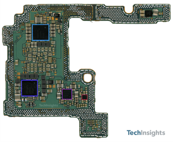
Basically, the whole product is in 2 packages. Not obvious how much smaller this could be made given the number of signals they want for the product.
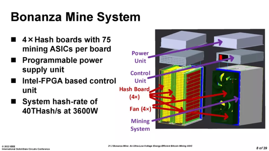
The next product I looked was the Intel Bitcoin mining chip / system. It is 7nm, but an interesting die size example. The design is based around the BZM1 chip. It is a 7 x 7.5mm exposed-die FCLGA package (132 balls). 300 of these chips power the system. Each chip die measures 4.14 x 3.42mm, for a total of 14.16mm^2 of silicon, so these are comparatively small slivers of silicon. The smaller die size improves yield and maximizes wafer area usage (up to 4,000 die per wafer), thus helping maximize production capacity (though it does require more wafer dicing/packaging capacity). Intel says these are 7nm ASICs, but doesn’t specify if that is its own ‘Intel 7,’ the original 7nm before it renamed the process node to ‘Intel 4,’ or TSMC’s 7nm process.
Other consumer devices
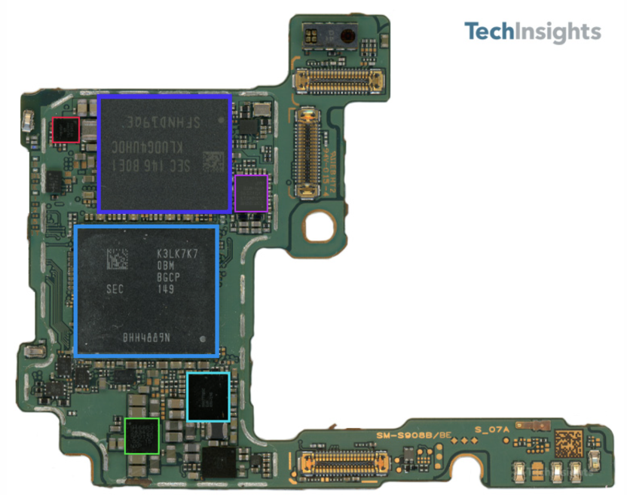
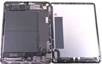
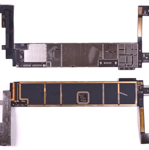
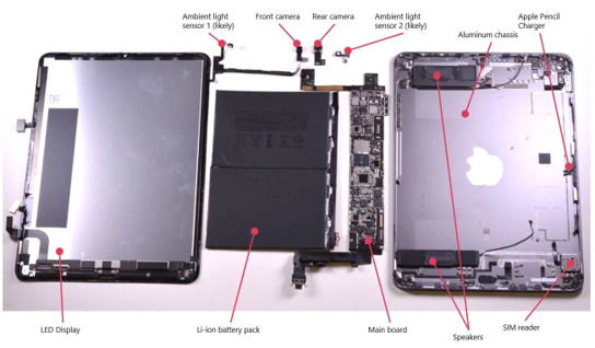
I then took a look at the latest Apple iPad Pro. It is very similar to the Samsung Galaxy 22 in chip count and integration approach.
So my light look into 5nm product electrical integration suggests that in core consumer applications (phones and pads) that there are not obvious choices to change integration strategy, but lower volume products with lower single die integration complexity seem to be well prepared for such an integration approach.
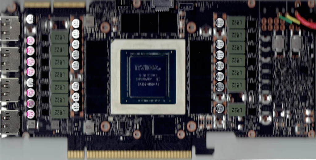
GPUs
While not a 5nm part, NVIDIAs leading edge A100 GPU has about 54 billion transistors and represents the performance people are looking at from 5nm parts. One of the major distinguishing differences between this part and those used in consumer level GPUs is memory.
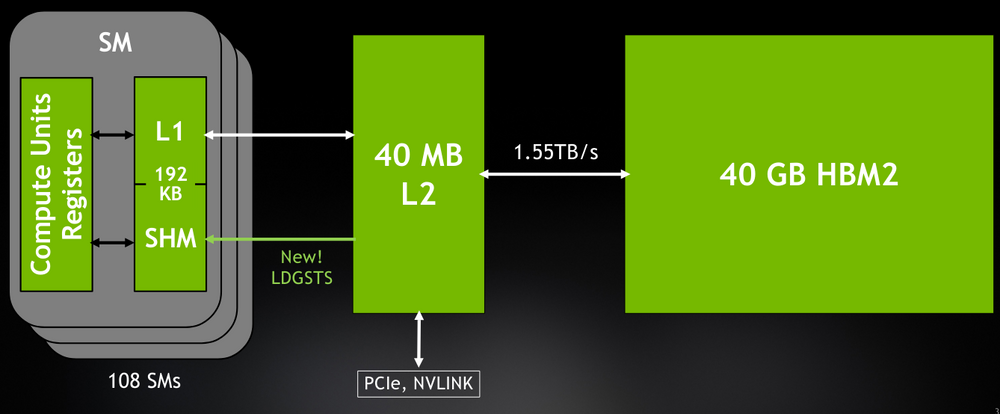
I couldn’t find a teardown of an A100 GPU (and at $32k each not surprised) I did find a few teardowns of consumer and professional level GPUs and they are pretty identical. As they lack HBM2 memory, they are unable to process as complex a model as the A100 can and suggests that the 7nm decision on these cards was probably fine.
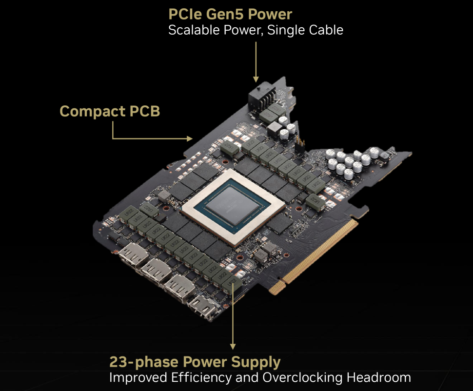
RTX 4090
RTX A5000